

Key Insights
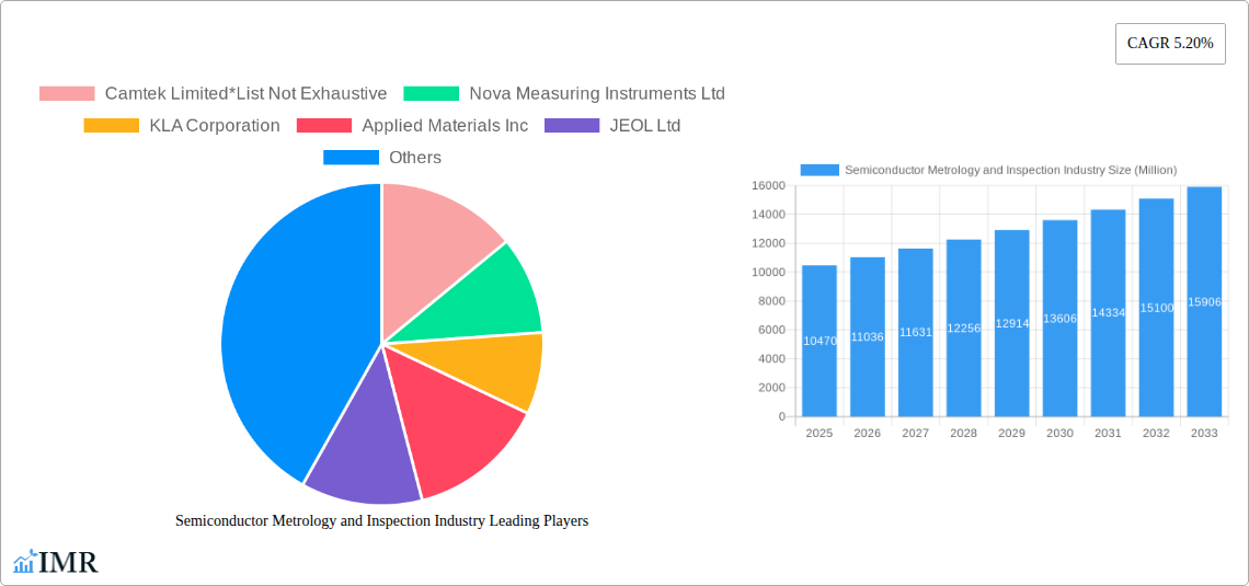
The semiconductor industry's relentless pursuit of miniaturization and performance enhancement fuels robust growth in the semiconductor metrology and inspection market. With a 2025 market size of $10.47 billion and a projected CAGR of 5.20% from 2025 to 2033, this sector is poised for significant expansion. Key drivers include the increasing complexity of semiconductor manufacturing processes, the rising demand for advanced node chips in diverse applications (like 5G, AI, and automotive electronics), and the stringent quality control requirements demanded by these advanced technologies. The market is segmented by type, encompassing lithography metrology, mask inspection and metrology, wafer inspection, thin film metrology, and other process control systems. Lithography metrology, crucial for ensuring the precision of chip patterns, is expected to maintain a significant market share, driven by the ongoing transition to EUV lithography and advanced patterning techniques. The demand for higher-resolution inspection systems, particularly for advanced nodes, is another key trend shaping the market. While challenges like high equipment costs and the need for skilled professionals exist, the overwhelming demand for sophisticated semiconductors will continuously outweigh these restraints, ensuring sustained market growth.
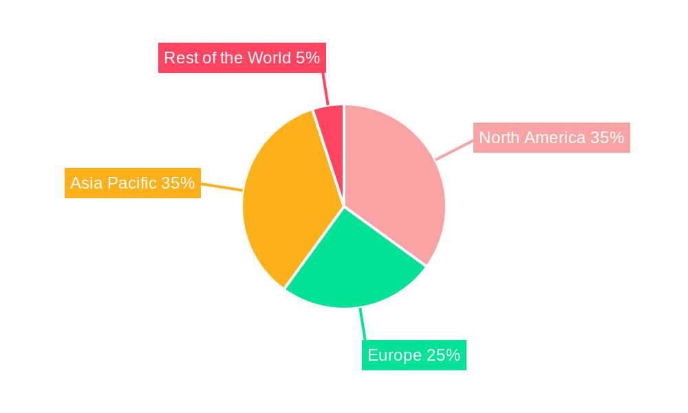
The competitive landscape is dominated by established players like KLA Corporation, Applied Materials, and ASML, who leverage their technological expertise and extensive customer relationships. However, the market also presents opportunities for smaller, specialized companies that offer niche solutions or innovative technologies. Regional growth will be largely influenced by the concentration of semiconductor manufacturing facilities. Asia-Pacific, fueled by substantial investments in semiconductor manufacturing capacity in countries like Taiwan, South Korea, and China, is anticipated to hold the largest market share. North America and Europe will retain significant market presence, driven by strong research and development activities and established manufacturing bases. The continued expansion of the semiconductor industry, particularly in areas like high-performance computing and automotive electronics, will ensure sustained demand for advanced metrology and inspection solutions, fostering significant growth and innovation in the coming decade.
Semiconductor Metrology and Inspection Market Report: 2019-2033
This comprehensive report provides a detailed analysis of the Semiconductor Metrology and Inspection industry, encompassing market dynamics, growth trends, regional analysis, competitive landscape, and future outlook. The study covers the period 2019-2033, with a focus on the forecast period 2025-2033 and a base year of 2025. The report is an invaluable resource for industry professionals, investors, and stakeholders seeking to understand this rapidly evolving market. Total market size in 2025 is estimated at xx Million.
Semiconductor Metrology and Inspection Industry Market Dynamics & Structure
The semiconductor metrology and inspection market is characterized by a moderately consolidated structure with a few key players holding significant market share. The market is driven by continuous technological advancements in semiconductor manufacturing, particularly in advanced nodes. Stringent regulatory frameworks governing semiconductor production and the increasing demand for higher-quality chips also fuel market growth. Competitive substitution primarily involves the introduction of more efficient and cost-effective inspection techniques. End-user demographics include leading semiconductor manufacturers across various regions, with a focus on advanced chip production facilities. M&A activities are frequent, driven by the need for companies to expand their product portfolios, technological capabilities, and market reach.
- Market Concentration: Highly concentrated, with top 5 players holding approximately xx% market share in 2025.
- Technological Innovation: Continuous advancements in AI, machine learning, and big data analytics are key drivers.
- Regulatory Landscape: Stringent regulations regarding safety and environmental standards impact manufacturing processes and equipment selection.
- Competitive Substitutes: Development of advanced optical inspection methods and alternative metrology technologies pose a competitive threat.
- M&A Activity: An average of xx M&A deals per year were observed during 2019-2024.
Semiconductor Metrology and Inspection Industry Growth Trends & Insights
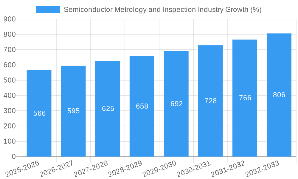
The semiconductor metrology and inspection market experienced substantial growth during the historical period (2019-2024), fueled by the rising demand for advanced semiconductor devices in various applications, such as 5G, AI, and high-performance computing. The market is projected to maintain a healthy Compound Annual Growth Rate (CAGR) of xx% during the forecast period (2025-2033). This growth is driven by several factors, including increasing adoption of advanced semiconductor manufacturing technologies, rising demand for smaller and faster chips, and the increasing complexity of semiconductor fabrication processes. Technological disruptions, such as the shift towards EUV lithography and the adoption of advanced packaging technologies, are further contributing to market growth. Consumer behavior shifts towards more sophisticated electronics are indirectly driving demand. Market penetration is increasing across various segments and regions, reaching approximately xx% in 2025.
Dominant Regions, Countries, or Segments in Semiconductor Metrology and Inspection Industry
The Asia-Pacific region, particularly Taiwan, South Korea, and China, dominates the semiconductor metrology and inspection market due to the high concentration of leading semiconductor manufacturers in these regions. North America also holds a significant market share. Within the segment breakdown:
- Lithography Metrology: This segment is experiencing the highest growth due to the increasing adoption of advanced lithographic techniques, such as EUV lithography.
- Wafer Inspection: This segment is also exhibiting strong growth due to the increasing demand for higher quality and yield in wafer manufacturing.
- Mask Inspection and Metrology: This is critical for high-yield chip production and is showing steady growth.
- Thin Film Metrology: Growth is driven by increasing complexity of thin film deposition processes.
- Other Process Control Systems: A smaller segment but with significant growth potential, driven by automation and process optimization.
Key Drivers:
- Strong government support for semiconductor industry development in key regions.
- Expansion of semiconductor fabrication plants and capacity increases.
- Continuous technological advancements in semiconductor manufacturing.
Semiconductor Metrology and Inspection Industry Product Landscape
The semiconductor metrology and inspection market offers a diverse range of products, including optical microscopes, scanning electron microscopes, atomic force microscopes, and various specialized software solutions for data analysis and process optimization. These products are characterized by high precision, advanced features, and increasing automation capabilities. Recent innovations focus on improving measurement accuracy, increasing throughput, and reducing inspection time. Key selling propositions revolve around enhanced resolution, improved data analysis tools, and seamless integration with existing manufacturing workflows.
Key Drivers, Barriers & Challenges in Semiconductor Metrology and Inspection Industry
Key Drivers:
- Growing demand for advanced semiconductor devices in various applications.
- Continuous technological advancements in semiconductor manufacturing processes.
- Government initiatives to promote domestic semiconductor manufacturing.
Key Challenges:
- High cost of advanced metrology and inspection equipment.
- Need for skilled personnel to operate and maintain sophisticated equipment.
- Intense competition among key players in the market. This leads to pricing pressure and a need for continuous innovation. The competitive landscape impacts margins and forces companies to adopt innovative strategies.
Emerging Opportunities in Semiconductor Metrology and Inspection Industry
Emerging opportunities lie in the development of advanced metrology and inspection techniques for next-generation semiconductor devices, including 3D chips and advanced packaging technologies. Further opportunities exist in expanding into emerging markets and leveraging artificial intelligence and machine learning for automated defect detection and process optimization.
Growth Accelerators in the Semiconductor Metrology and Inspection Industry Industry
Long-term growth is fueled by technological breakthroughs in areas such as AI-driven defect detection and advanced imaging techniques. Strategic partnerships between metrology equipment suppliers and semiconductor manufacturers are accelerating adoption and driving innovation. Expanding into new applications, particularly in emerging markets, promises significant growth opportunities.
Key Players Shaping the Semiconductor Metrology and Inspection Industry Market
- Camtek Limited
- Nova Measuring Instruments Ltd
- KLA Corporation
- Applied Materials Inc
- JEOL Ltd
- Hitachi Hi-Technologies Corporation (Hitachi Limited)
- Lasertec Corporation
- Nikon Metrology NV (Nikon Group)
- Thermo Fisher Scientific Inc
- Onto Innovation Inc
- ASML Holding NV
Notable Milestones in Semiconductor Metrology and Inspection Industry Sector
- 2021-Q3: KLA Corporation launched its new advanced optical inspection system.
- 2022-Q1: Applied Materials acquired a smaller metrology company, expanding its portfolio.
- 2023-Q2: ASML announced significant advancements in EUV lithography metrology. (Specific details would need to be filled in with actual events)
In-Depth Semiconductor Metrology and Inspection Industry Market Outlook
The semiconductor metrology and inspection market is poised for significant growth over the next decade. Continuous advancements in semiconductor technology and the increasing demand for advanced semiconductor devices will drive demand for sophisticated metrology and inspection solutions. Strategic partnerships, technological breakthroughs, and expansion into new markets will be key factors in shaping future market dynamics. The potential for market expansion into new applications and regions promises considerable long-term growth.
Semiconductor Metrology and Inspection Industry Segmentation
-
1. Type
-
1.1. Lithography Metrology
- 1.1.1. Overlay
- 1.1.2. Dimension Equipment
- 1.1.3. Mask Inspection and Metrology
- 1.2. Wafer Inspection
- 1.3. Thin Film Metrology
- 1.4. Other Process Control Systems
-
1.1. Lithography Metrology
Semiconductor Metrology and Inspection Industry Segmentation By Geography
- 1. North America
- 2. Europe
- 3. Asia Pacific
- 4. Rest of the World
Semiconductor Metrology and Inspection Industry REPORT HIGHLIGHTS
| Aspects | Details |
|---|---|
| Study Period | 2019-2033 |
| Base Year | 2024 |
| Estimated Year | 2025 |
| Forecast Period | 2025-2033 |
| Historical Period | 2019-2024 |
| Growth Rate | CAGR of 5.20% from 2019-2033 |
| Segmentation |
|
Table of Contents
- 1. Introduction
- 1.1. Research Scope
- 1.2. Market Segmentation
- 1.3. Research Methodology
- 1.4. Definitions and Assumptions
- 2. Executive Summary
- 2.1. Introduction
- 3. Market Dynamics
- 3.1. Introduction
- 3.2. Market Drivers
- 3.2.1 Increasing Demand for High-performance
- 3.2.2 Low-cost Semiconductors; Increasing Demand for Semiconductor Wafers in Consumer Electronics
- 3.3. Market Restrains
- 3.3.1. High Setup Cost and Lack of Expertise in Handling Metrology Systems Efficiently; High Raw Material and Fabrication Costs
- 3.4. Market Trends
- 3.4.1. Wafer Inspection to Witness Significant Growth
- 4. Market Factor Analysis
- 4.1. Porters Five Forces
- 4.2. Supply/Value Chain
- 4.3. PESTEL analysis
- 4.4. Market Entropy
- 4.5. Patent/Trademark Analysis
- 5. Global Semiconductor Metrology and Inspection Industry Analysis, Insights and Forecast, 2019-2031
- 5.1. Market Analysis, Insights and Forecast - by Type
- 5.1.1. Lithography Metrology
- 5.1.1.1. Overlay
- 5.1.1.2. Dimension Equipment
- 5.1.1.3. Mask Inspection and Metrology
- 5.1.2. Wafer Inspection
- 5.1.3. Thin Film Metrology
- 5.1.4. Other Process Control Systems
- 5.1.1. Lithography Metrology
- 5.2. Market Analysis, Insights and Forecast - by Region
- 5.2.1. North America
- 5.2.2. Europe
- 5.2.3. Asia Pacific
- 5.2.4. Rest of the World
- 5.1. Market Analysis, Insights and Forecast - by Type
- 6. North America Semiconductor Metrology and Inspection Industry Analysis, Insights and Forecast, 2019-2031
- 6.1. Market Analysis, Insights and Forecast - by Type
- 6.1.1. Lithography Metrology
- 6.1.1.1. Overlay
- 6.1.1.2. Dimension Equipment
- 6.1.1.3. Mask Inspection and Metrology
- 6.1.2. Wafer Inspection
- 6.1.3. Thin Film Metrology
- 6.1.4. Other Process Control Systems
- 6.1.1. Lithography Metrology
- 6.1. Market Analysis, Insights and Forecast - by Type
- 7. Europe Semiconductor Metrology and Inspection Industry Analysis, Insights and Forecast, 2019-2031
- 7.1. Market Analysis, Insights and Forecast - by Type
- 7.1.1. Lithography Metrology
- 7.1.1.1. Overlay
- 7.1.1.2. Dimension Equipment
- 7.1.1.3. Mask Inspection and Metrology
- 7.1.2. Wafer Inspection
- 7.1.3. Thin Film Metrology
- 7.1.4. Other Process Control Systems
- 7.1.1. Lithography Metrology
- 7.1. Market Analysis, Insights and Forecast - by Type
- 8. Asia Pacific Semiconductor Metrology and Inspection Industry Analysis, Insights and Forecast, 2019-2031
- 8.1. Market Analysis, Insights and Forecast - by Type
- 8.1.1. Lithography Metrology
- 8.1.1.1. Overlay
- 8.1.1.2. Dimension Equipment
- 8.1.1.3. Mask Inspection and Metrology
- 8.1.2. Wafer Inspection
- 8.1.3. Thin Film Metrology
- 8.1.4. Other Process Control Systems
- 8.1.1. Lithography Metrology
- 8.1. Market Analysis, Insights and Forecast - by Type
- 9. Rest of the World Semiconductor Metrology and Inspection Industry Analysis, Insights and Forecast, 2019-2031
- 9.1. Market Analysis, Insights and Forecast - by Type
- 9.1.1. Lithography Metrology
- 9.1.1.1. Overlay
- 9.1.1.2. Dimension Equipment
- 9.1.1.3. Mask Inspection and Metrology
- 9.1.2. Wafer Inspection
- 9.1.3. Thin Film Metrology
- 9.1.4. Other Process Control Systems
- 9.1.1. Lithography Metrology
- 9.1. Market Analysis, Insights and Forecast - by Type
- 10. North America Semiconductor Metrology and Inspection Industry Analysis, Insights and Forecast, 2019-2031
- 10.1. Market Analysis, Insights and Forecast - By Country/Sub-region
- 10.1.1.
- 11. Europe Semiconductor Metrology and Inspection Industry Analysis, Insights and Forecast, 2019-2031
- 11.1. Market Analysis, Insights and Forecast - By Country/Sub-region
- 11.1.1.
- 12. Asia Pacific Semiconductor Metrology and Inspection Industry Analysis, Insights and Forecast, 2019-2031
- 12.1. Market Analysis, Insights and Forecast - By Country/Sub-region
- 12.1.1.
- 13. Rest of the World Semiconductor Metrology and Inspection Industry Analysis, Insights and Forecast, 2019-2031
- 13.1. Market Analysis, Insights and Forecast - By Country/Sub-region
- 13.1.1.
- 14. Competitive Analysis
- 14.1. Global Market Share Analysis 2024
- 14.2. Company Profiles
- 14.2.1 Camtek Limited*List Not Exhaustive
- 14.2.1.1. Overview
- 14.2.1.2. Products
- 14.2.1.3. SWOT Analysis
- 14.2.1.4. Recent Developments
- 14.2.1.5. Financials (Based on Availability)
- 14.2.2 Nova Measuring Instruments Ltd
- 14.2.2.1. Overview
- 14.2.2.2. Products
- 14.2.2.3. SWOT Analysis
- 14.2.2.4. Recent Developments
- 14.2.2.5. Financials (Based on Availability)
- 14.2.3 KLA Corporation
- 14.2.3.1. Overview
- 14.2.3.2. Products
- 14.2.3.3. SWOT Analysis
- 14.2.3.4. Recent Developments
- 14.2.3.5. Financials (Based on Availability)
- 14.2.4 Applied Materials Inc
- 14.2.4.1. Overview
- 14.2.4.2. Products
- 14.2.4.3. SWOT Analysis
- 14.2.4.4. Recent Developments
- 14.2.4.5. Financials (Based on Availability)
- 14.2.5 JEOL Ltd
- 14.2.5.1. Overview
- 14.2.5.2. Products
- 14.2.5.3. SWOT Analysis
- 14.2.5.4. Recent Developments
- 14.2.5.5. Financials (Based on Availability)
- 14.2.6 Hitachi Hi-Technologies Corporation (Hitachi Limited)
- 14.2.6.1. Overview
- 14.2.6.2. Products
- 14.2.6.3. SWOT Analysis
- 14.2.6.4. Recent Developments
- 14.2.6.5. Financials (Based on Availability)
- 14.2.7 Lasertec Corporation
- 14.2.7.1. Overview
- 14.2.7.2. Products
- 14.2.7.3. SWOT Analysis
- 14.2.7.4. Recent Developments
- 14.2.7.5. Financials (Based on Availability)
- 14.2.8 Nikon Metrology NV (Nikon Group)
- 14.2.8.1. Overview
- 14.2.8.2. Products
- 14.2.8.3. SWOT Analysis
- 14.2.8.4. Recent Developments
- 14.2.8.5. Financials (Based on Availability)
- 14.2.9 Thermo Fisher Scientific Inc
- 14.2.9.1. Overview
- 14.2.9.2. Products
- 14.2.9.3. SWOT Analysis
- 14.2.9.4. Recent Developments
- 14.2.9.5. Financials (Based on Availability)
- 14.2.10 Onto Innovation Inc
- 14.2.10.1. Overview
- 14.2.10.2. Products
- 14.2.10.3. SWOT Analysis
- 14.2.10.4. Recent Developments
- 14.2.10.5. Financials (Based on Availability)
- 14.2.11 ASML Holding NV
- 14.2.11.1. Overview
- 14.2.11.2. Products
- 14.2.11.3. SWOT Analysis
- 14.2.11.4. Recent Developments
- 14.2.11.5. Financials (Based on Availability)
- 14.2.1 Camtek Limited*List Not Exhaustive
List of Figures
- Figure 1: Global Semiconductor Metrology and Inspection Industry Revenue Breakdown (Million, %) by Region 2024 & 2032
- Figure 2: North America Semiconductor Metrology and Inspection Industry Revenue (Million), by Country 2024 & 2032
- Figure 3: North America Semiconductor Metrology and Inspection Industry Revenue Share (%), by Country 2024 & 2032
- Figure 4: Europe Semiconductor Metrology and Inspection Industry Revenue (Million), by Country 2024 & 2032
- Figure 5: Europe Semiconductor Metrology and Inspection Industry Revenue Share (%), by Country 2024 & 2032
- Figure 6: Asia Pacific Semiconductor Metrology and Inspection Industry Revenue (Million), by Country 2024 & 2032
- Figure 7: Asia Pacific Semiconductor Metrology and Inspection Industry Revenue Share (%), by Country 2024 & 2032
- Figure 8: Rest of the World Semiconductor Metrology and Inspection Industry Revenue (Million), by Country 2024 & 2032
- Figure 9: Rest of the World Semiconductor Metrology and Inspection Industry Revenue Share (%), by Country 2024 & 2032
- Figure 10: North America Semiconductor Metrology and Inspection Industry Revenue (Million), by Type 2024 & 2032
- Figure 11: North America Semiconductor Metrology and Inspection Industry Revenue Share (%), by Type 2024 & 2032
- Figure 12: North America Semiconductor Metrology and Inspection Industry Revenue (Million), by Country 2024 & 2032
- Figure 13: North America Semiconductor Metrology and Inspection Industry Revenue Share (%), by Country 2024 & 2032
- Figure 14: Europe Semiconductor Metrology and Inspection Industry Revenue (Million), by Type 2024 & 2032
- Figure 15: Europe Semiconductor Metrology and Inspection Industry Revenue Share (%), by Type 2024 & 2032
- Figure 16: Europe Semiconductor Metrology and Inspection Industry Revenue (Million), by Country 2024 & 2032
- Figure 17: Europe Semiconductor Metrology and Inspection Industry Revenue Share (%), by Country 2024 & 2032
- Figure 18: Asia Pacific Semiconductor Metrology and Inspection Industry Revenue (Million), by Type 2024 & 2032
- Figure 19: Asia Pacific Semiconductor Metrology and Inspection Industry Revenue Share (%), by Type 2024 & 2032
- Figure 20: Asia Pacific Semiconductor Metrology and Inspection Industry Revenue (Million), by Country 2024 & 2032
- Figure 21: Asia Pacific Semiconductor Metrology and Inspection Industry Revenue Share (%), by Country 2024 & 2032
- Figure 22: Rest of the World Semiconductor Metrology and Inspection Industry Revenue (Million), by Type 2024 & 2032
- Figure 23: Rest of the World Semiconductor Metrology and Inspection Industry Revenue Share (%), by Type 2024 & 2032
- Figure 24: Rest of the World Semiconductor Metrology and Inspection Industry Revenue (Million), by Country 2024 & 2032
- Figure 25: Rest of the World Semiconductor Metrology and Inspection Industry Revenue Share (%), by Country 2024 & 2032
List of Tables
- Table 1: Global Semiconductor Metrology and Inspection Industry Revenue Million Forecast, by Region 2019 & 2032
- Table 2: Global Semiconductor Metrology and Inspection Industry Revenue Million Forecast, by Type 2019 & 2032
- Table 3: Global Semiconductor Metrology and Inspection Industry Revenue Million Forecast, by Region 2019 & 2032
- Table 4: Global Semiconductor Metrology and Inspection Industry Revenue Million Forecast, by Country 2019 & 2032
- Table 5: Semiconductor Metrology and Inspection Industry Revenue (Million) Forecast, by Application 2019 & 2032
- Table 6: Global Semiconductor Metrology and Inspection Industry Revenue Million Forecast, by Country 2019 & 2032
- Table 7: Semiconductor Metrology and Inspection Industry Revenue (Million) Forecast, by Application 2019 & 2032
- Table 8: Global Semiconductor Metrology and Inspection Industry Revenue Million Forecast, by Country 2019 & 2032
- Table 9: Semiconductor Metrology and Inspection Industry Revenue (Million) Forecast, by Application 2019 & 2032
- Table 10: Global Semiconductor Metrology and Inspection Industry Revenue Million Forecast, by Country 2019 & 2032
- Table 11: Semiconductor Metrology and Inspection Industry Revenue (Million) Forecast, by Application 2019 & 2032
- Table 12: Global Semiconductor Metrology and Inspection Industry Revenue Million Forecast, by Type 2019 & 2032
- Table 13: Global Semiconductor Metrology and Inspection Industry Revenue Million Forecast, by Country 2019 & 2032
- Table 14: Global Semiconductor Metrology and Inspection Industry Revenue Million Forecast, by Type 2019 & 2032
- Table 15: Global Semiconductor Metrology and Inspection Industry Revenue Million Forecast, by Country 2019 & 2032
- Table 16: Global Semiconductor Metrology and Inspection Industry Revenue Million Forecast, by Type 2019 & 2032
- Table 17: Global Semiconductor Metrology and Inspection Industry Revenue Million Forecast, by Country 2019 & 2032
- Table 18: Global Semiconductor Metrology and Inspection Industry Revenue Million Forecast, by Type 2019 & 2032
- Table 19: Global Semiconductor Metrology and Inspection Industry Revenue Million Forecast, by Country 2019 & 2032
Frequently Asked Questions
1. What is the projected Compound Annual Growth Rate (CAGR) of the Semiconductor Metrology and Inspection Industry?
The projected CAGR is approximately 5.20%.
2. Which companies are prominent players in the Semiconductor Metrology and Inspection Industry?
Key companies in the market include Camtek Limited*List Not Exhaustive, Nova Measuring Instruments Ltd, KLA Corporation, Applied Materials Inc, JEOL Ltd, Hitachi Hi-Technologies Corporation (Hitachi Limited), Lasertec Corporation, Nikon Metrology NV (Nikon Group), Thermo Fisher Scientific Inc, Onto Innovation Inc, ASML Holding NV.
3. What are the main segments of the Semiconductor Metrology and Inspection Industry?
The market segments include Type.
4. Can you provide details about the market size?
The market size is estimated to be USD 10.47 Million as of 2022.
5. What are some drivers contributing to market growth?
Increasing Demand for High-performance. Low-cost Semiconductors; Increasing Demand for Semiconductor Wafers in Consumer Electronics.
6. What are the notable trends driving market growth?
Wafer Inspection to Witness Significant Growth.
7. Are there any restraints impacting market growth?
High Setup Cost and Lack of Expertise in Handling Metrology Systems Efficiently; High Raw Material and Fabrication Costs.
8. Can you provide examples of recent developments in the market?
N/A
9. What pricing options are available for accessing the report?
Pricing options include single-user, multi-user, and enterprise licenses priced at USD 4750, USD 5250, and USD 8750 respectively.
10. Is the market size provided in terms of value or volume?
The market size is provided in terms of value, measured in Million.
11. Are there any specific market keywords associated with the report?
Yes, the market keyword associated with the report is "Semiconductor Metrology and Inspection Industry," which aids in identifying and referencing the specific market segment covered.
12. How do I determine which pricing option suits my needs best?
The pricing options vary based on user requirements and access needs. Individual users may opt for single-user licenses, while businesses requiring broader access may choose multi-user or enterprise licenses for cost-effective access to the report.
13. Are there any additional resources or data provided in the Semiconductor Metrology and Inspection Industry report?
While the report offers comprehensive insights, it's advisable to review the specific contents or supplementary materials provided to ascertain if additional resources or data are available.
14. How can I stay updated on further developments or reports in the Semiconductor Metrology and Inspection Industry?
To stay informed about further developments, trends, and reports in the Semiconductor Metrology and Inspection Industry, consider subscribing to industry newsletters, following relevant companies and organizations, or regularly checking reputable industry news sources and publications.
Methodology
Step 1 - Identification of Relevant Samples Size from Population Database


Step 2 - Approaches for Defining Global Market Size (Value, Volume* & Price*)

Note*: In applicable scenarios
Step 3 - Data Sources
Primary Research
- Web Analytics
- Survey Reports
- Research Institute
- Latest Research Reports
- Opinion Leaders
Secondary Research
- Annual Reports
- White Paper
- Latest Press Release
- Industry Association
- Paid Database
- Investor Presentations

Step 4 - Data Triangulation
Involves using different sources of information in order to increase the validity of a study
These sources are likely to be stakeholders in a program - participants, other researchers, program staff, other community members, and so on.
Then we put all data in single framework & apply various statistical tools to find out the dynamic on the market.
During the analysis stage, feedback from the stakeholder groups would be compared to determine areas of agreement as well as areas of divergence
